What is PCB Design? A Complete Guide to PCB Design Services
Printed Circuit Boards (PCBs) are the heart of modern electrical gadgets. Almost every electrical product, from cellphones and industrial machinery to medical gadgets and automobile systems, needs a PCB to work effectively.
In an era of ever-smaller and more sophisticated products, knowledge of PCB design has become increasingly crucial for product businesses, manufacturers, and supply chain leaders. Many people starting out in a career in hardware development raise the question: What is PCB design and how does it fit into the broader product development process?
To put it simply, PCB design is the process of turning an electronic circuit into a physical board that can be manufactured and used in the real world. A well-designed PCB goes a long way in ensuring the finished product is efficient, reliable, and scalable.
This article describes the basics of PCB design, its important stages, and why PCB design services are important for successful electronics product development.
The Foundation of Modern Electronics
Before talking about the design process, it is vital to understand what is PCB in electronics.
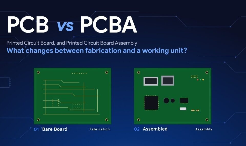
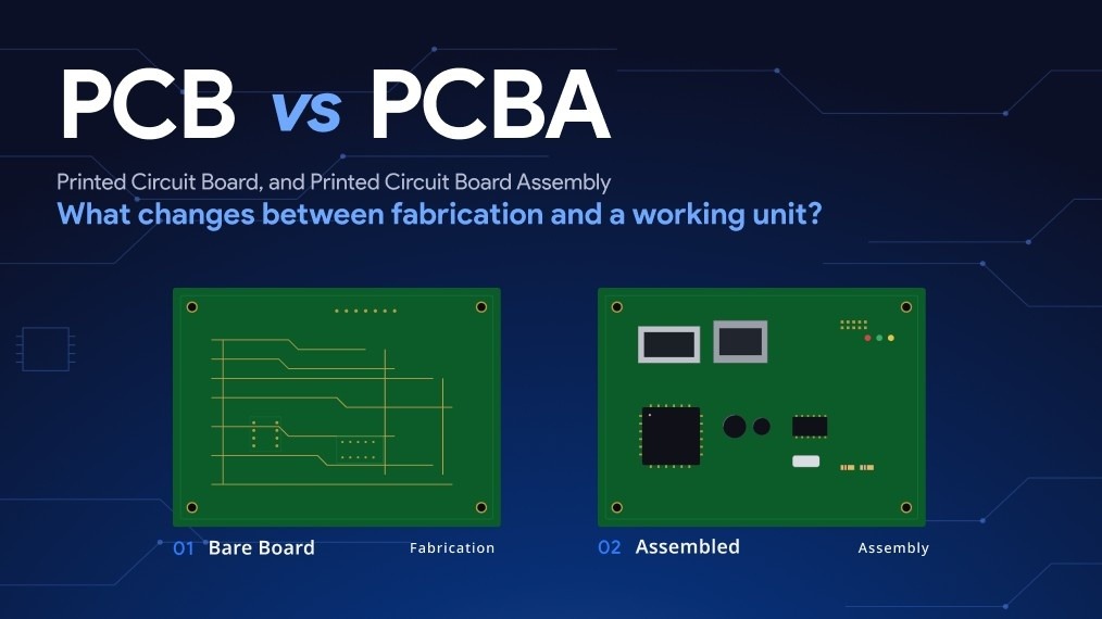
A Printed Circuit Board (PCB) is a board that mechanically supports and electrically links electronic components using conductive tracks. The components are placed directly on the board instead of using lots of cables. This makes for a reliable and compact electrical system.
PCBs are used in nearly every electronic product, including:
- Industrial automation systems
- Smart home devices
- Medical equipment
- Automotive electronics
- Consumer products
As products become smaller and more advanced, PCB design and development have become a critical part of engineering and manufacturing success.
What is PCB Designing: From Circuit Concept to Product Reality
Many people entering hardware development wonder what PCB designing is and how it differs from creating an electronic circuit.
PCB designing is the process of taking a circuit schematic diagram and translating it into a physical layout on a board that can be manufactured and installed efficiently. The engineer's role is to guarantee that the board works reliably and meets production, cost, and compliance requirements.
Modern PCB design services go beyond simply connecting components. They consider:
- Signal integrity
- Thermal management
- Electromagnetic interference (EMI)
- Design for Manufacturing and Assembly (DFMA)
- Testing requirements
- Component availability
For example, industrial equipment that is interconnected and designed to work in extreme settings requires a circuit board that can endure heat, electrical interference, and continuous operation. Likewise, EVs demand high durability in conditions of vibration and temperature changes, and fintech hardware like payment terminals require small, secure, and extremely dependable PCB designs. These requirements must be considered during the design stage rather than after production begins.
PCB Design Services India: The Key Stages of PCB Development
A successful PCB assembly follows a structured engineering process.
1. Schematic Design
First, you design a circuit schematic. It shows all the electronic components and their electrical interconnections. Component selection and BOM optimization are often conducted at this stage to avoid sourcing complications down the road.
2. Component Placement
The components are properly placed on the PCB in order to enhance signal integrity, heat dissipation, and assembly. Proper placement makes the design easier.
3. Layout and Routing
Engineers create the physical electrical pathways that connect components. Trace widths, power distribution, and grounding strategies are carefully planned to ensure stable performance.
4. Verification and Prototyping
Prior to PCB assembly, the design goes through simulations and design rule checking. Boards are prototyped and tested to catch any problems before full manufacturing.
Why PCB Design Impacts Business Performance?
PCB design is not just an engineering activity. It directly affects business outcomes. This is particularly important for industries such as electric vehicles and fintech, where delayed certifications, component shortages, or multiple redesigns can significantly impact product launch schedules and overall project costs.
Poor design can lead to:
- Product failures
- Low manufacturing yields
- Higher assembly or redesign costs
- Delayed product launches
- Increased warranty claims
For procurement teams and supply chain leaders, design choices early in the development cycle also impact component sourcing, long-term availability and manufacturing costs. If the PCB is not designed correctly and the DFMA or component lifetime risks are not taken into account, there might be delays in procurement, increased BOM prices, and bottlenecks in manufacturing.
However, a good PCB design and assembly process will enhance manufacturability, decrease production risks, optimize procurement, and speed up the time-to-market process. Through addressing engineering and sourcing issues upfront, organizations can avoid expensive redesigns, sustain reliable production schedules, and ensure low total cost of ownership throughout the product lifecycle.
Common Challenges in PCB Development
As electronic devices are becoming more complicated, companies encounter many issues related to design.
1. Supply Chain Constraints
A lack of components and their obsolescence might lead to delays in production. Engineers have to take into account availability when choosing components.
2. Thermal Management
Excessive heat can reduce performance and shorten product lifespan. Proper thermal planning helps maintain reliability and product quality.
3. Product Miniaturization
Modern products are expected to deliver more functionality in smaller form factors. This increases design complexity and requires careful engineering decisions.
4. Regulatory Compliance
There are certain products that are required to meet various standards, such as CE, FCC, and RoHS. The incorporation of these standards during the design process ensures that the certification process does not delay, and any redesigning will be avoided.
How Elecbits Helps Turn Electronic Ideas into Market-Ready Products
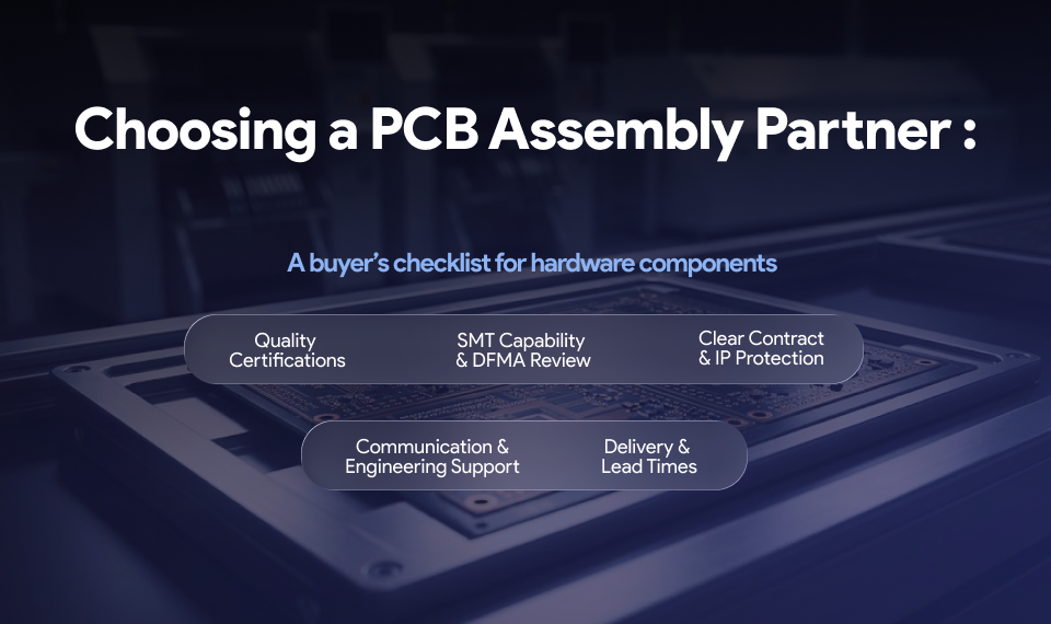
If you're evaluating PCB design services, look beyond circuit design capabilities. The right partner should help reduce engineering risks, optimize procurement, and ensure your product is ready for scalable manufacturing.
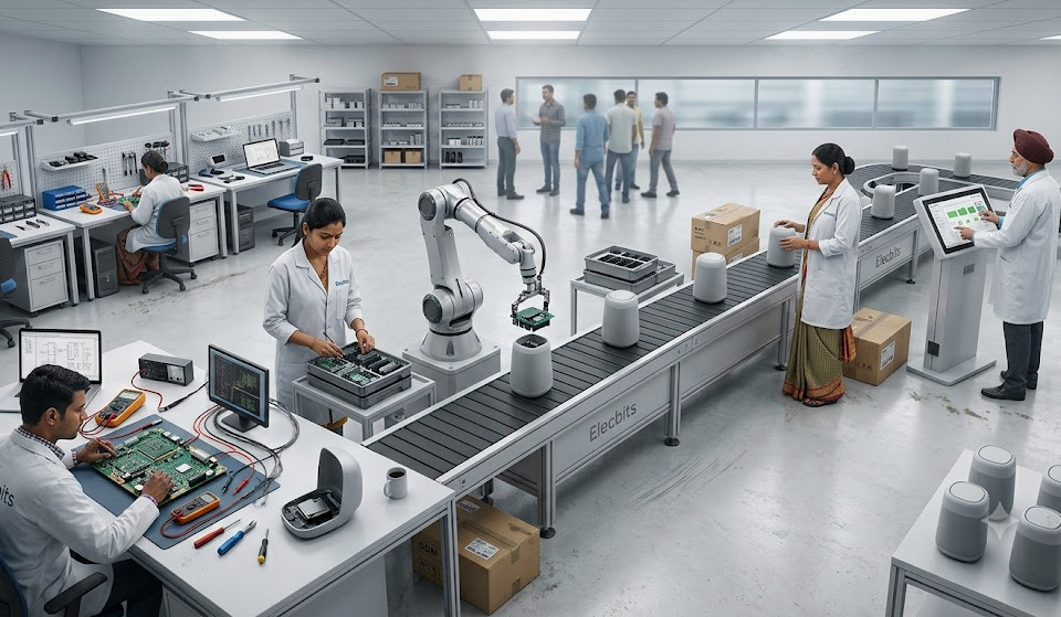
Elecbits provides end-to-end electronic product development, covering PCB design, embedded systems engineering, firmware development, industrial design, testing, DFMA implementation, PCB assembly, and turnkey manufacturing. To help businesses make better engineering and sourcing decisions, Elecbits has developed Elecbits XOR, an industry-first AI-powered electronics engineering and manufacturing platform that delivers instant quotations, intelligent BOM optimization, real-time component visibility, transparent supply chain insights, and proactive risk management. This enables manufacturers to make faster, risk-informed sourcing decisions, minimize component-related disruptions, and accelerate product development with greater confidence.
Whether you're developing a new electronic product or planning for volume manufacturing, Elecbits combines technical knowledge and AI-powered supply chain intelligence to help you bring products to market faster, more efficiently, and with less overall risk.
Conclusion
PCB design and assembly is much more than placing components on the circuit board; it is an intricate strategy that determines the effectiveness of the product, the efficiency of manufacturing, reliability, and the future success of the company.
With the constant evolution of electronic products, companies need to be prepared for development in mind and with a perspective on manufacturability, testability, compliance, and scalability. Early implementation of advanced PCB design solutions will definitely help companies mitigate potential risks and produce successful products.
Nowadays, in a highly competitive world of electronics, good PCB design is not just an engineering necessity but also a competitive advantage.



 Resources Quality standards Reliable methods to keep our quality consistent. Blog Deep dive into market-moving trends.