Where Most Things Usually Go Wrong
A founder submits a Gerber file expecting finished boards with components attached, but the vendor only supplies bare boards. Another team finalizes a BOM (Bill of Materials) without checking availability, and the assembly gets delayed.
This gap ultimately comes down to people's view of PCB fabrication and assembly process. They sound alike, but they handle completely different challenges.
What is PCB Fabrication?
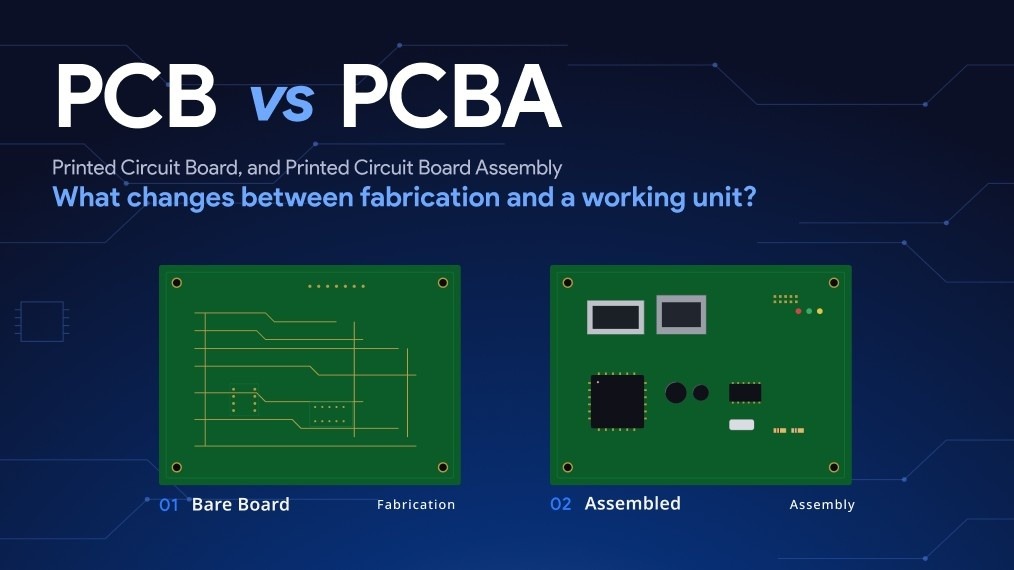
PCB fabrication is the process of creating a bare printed circuit board by forming layers, copper traces, vias, and surfaces based on design files, without adding electronic components.
This process includes:
- Selecting materials and layer stack-up
- Etching copper traces
- Drilling holes and vias
- Applying solder mask and silkscreen
At this point, the board has no components. It merely defines the electrical pathway. The choice of trace width, layer count, and material selection is a key factor for teams working on PCB design and fabrication, and has a direct impact on performance, especially for high-speed or power-sensitive applications.
What is PCB Assembly?
PCB assembly is the process of mounting and soldering electronic components on the manufactured board using either automated or manual processes.
Key steps include:
- Sourcing components based on the BOM
- Pick-and-place for SMT components
- Through-hole insertion if needed
- Soldering and inspection
- Functional testing
Once the assembly process is complete, the PCB turns into a fully operational electronic circuit whereby all its parts work together to deliver the desired functionality.
Difference between PCB Fabrication and Assembly
Understanding what is the difference between PCB assembly and fabrication is critical, especially when scaling production.
1. Role in the Product Lifecycle
PCB fabrication is the initial stage. It takes your design files and makes a physical bare board with copper traces, layers, and drilled holes. Without this step, there's nothing to assemble.
The next step is the PCB assembly, where the components are mounted and soldered to make the board functional. PCB fabrication defines the structure, and assembly makes the circuit functional. Any delays in the fabrication process push everything downstream.
2. Data and Inputs
PCB Fabrication is based on design outputs such as Gerber files, drill files, stack-up information, and material specifications. They determine the arrangement and physical structure of the board.
For PCB assembly, you need a different set of inputs: BOM (Bill of Materials), pick-and-place files, and assembly drawings. It also depends on accurate component sourcing. Any discrepancy between these files can result in bad builds or stop production.
3. Equipment and Expertise
The PCB fabrication process requires extensive manufacturing activities such as etching, laminating, drilling, and plating. The fabrication process requires special factories and process control. In contrast, assembly utilizes SMT machines, reflow ovens, and inspection equipment.
The skill set needed for both PCB fabrication vs assembly is very different. Fabrication is related to material and structure, while assembly ensures placement precision and electrical performance.
4. Failure Impact
Fabrication defects have an impact on the entire board, including issues like damaged traces, misaligned layers, poor quality materials, and more. Assembly defects are generally component-related defects.
Examples include misaligned components, solder bridging, and missing components. Some assembly problems can be fixed, but fabrication flaws can't. Mistakes in fabrication are thus more costly and more difficult to recover from.
5. Cost and Scalability
The cost of fabrication depends on how complicated the boards are, the number of layers, the materials used, and the volume. After setting up, scaling the fabrication process is fairly predictable. The cost of assembly is dependent on the number of components, sourcing, and the amount of manual or automated labor required. High-mix, low-volume builds make assembly more complex and expensive.
As you scale, optimizing assembly becomes crucial, because component placement, sourcing delays and yield rates have a direct impact on production speed and margins.
PCB Fabrication vs PCB Assembly: Comparison Table
| Aspect |
PCB Fabrication |
PCB Assembly |
| Purpose |
Builds the physical board |
Adds components to make it functional |
| Input Data |
Gerber files, drill files, stack-up |
BOM, pick-and-place files, schematics |
| Key Standards |
IPC-6012, IPC-A-600 |
IPC-A-610, J-STD-001 |
| Process Type |
Chemical and mechanical processes |
Mechanical and thermal processes |
| Equipment |
Etching machines, CNC drills, lamination presses |
Pick-and-place machines, reflow ovens |
| Output |
Bare PCB |
Fully assembled PCB |
| Error Impact |
Board must be scrapped and remade |
Often fixable with rework |
| Cost Drivers |
Material, layer count, complexity |
Components, sourcing, assembly complexity |
| Scalability |
Becomes cheaper in volume |
Costs vary with BOM and supply chain |
How Elecbits Helps You Move from Design to Production Without Delays
If PCB fabrication and assembly are managed by several different vendors the problems will arise; poor communication, delays in schedules, and everything becomes harder to track.
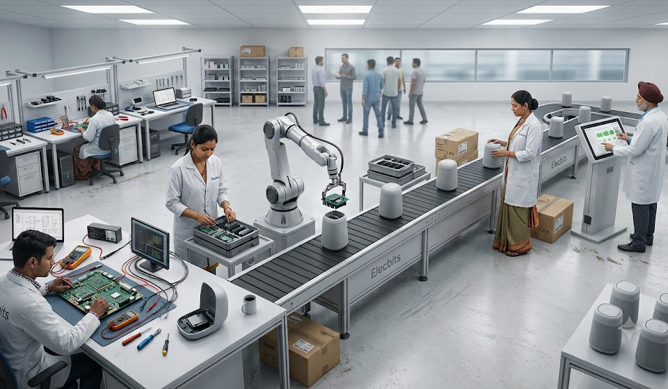
However, Elecbits ensures a streamlined process that encompasses all three phases of PCB production in one operation, making it easier for startups and businesses. Teams get better supply chain visibility, faster turnaround, and fewer coordination concerns.
With Elecbits, you can do it all, PCB design and fabrication to assembly in one spot, instead of having to chase down various vendors to get updates on components and assembly. This reduces delays caused by missing parts or incorrect specifications and helps maintain uniformity from batch to batch.
Conclusion
Hardware manufacturing is optimal if all processes are well-defined. PCB fabrication and assembly are related processes, but they play different roles. Once you understand both processes, effective planning and implementation are easy.
This makes the job much easier for startups and product development teams. This also ensures that companies build a robust foundation for consistent, scalable manufacturing.


 Resources Quality standards Reliable methods to keep our quality consistent. Blog Deep dive into market-moving trends.