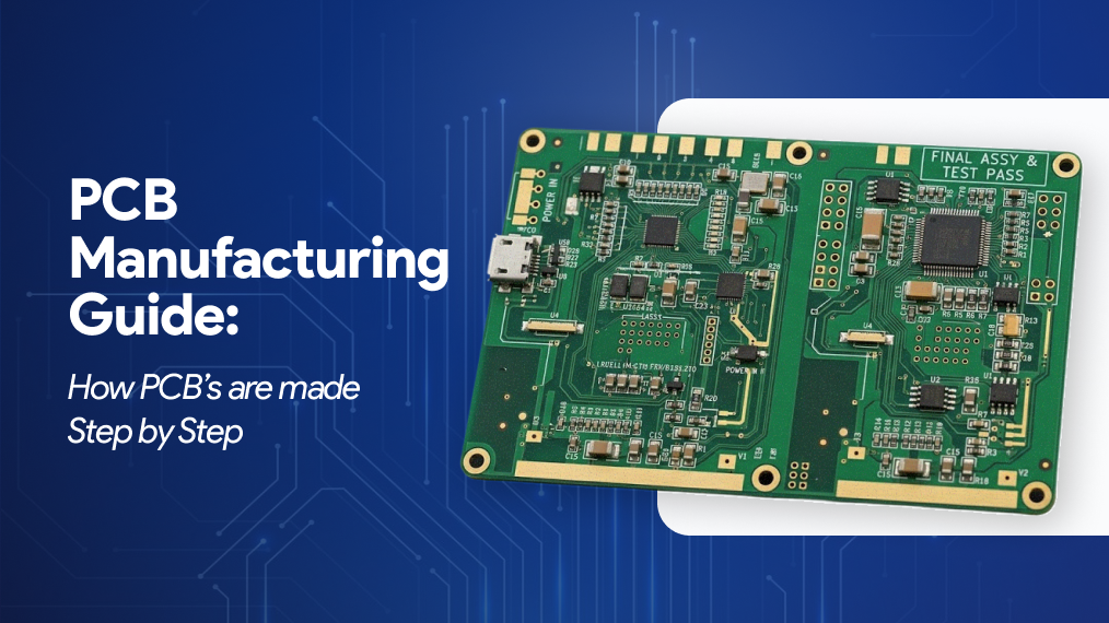
Ever wondered how a PCB goes from a digital circuit design to a fully manufactured board? It's much more than just printing copper on a surface. The PCB manufacturing process involves numerous steps, including imaging, etching, drilling, copper plating, solder masking, and electrical testing to prepare the board for assembly. This is the process on which the entire electronic product relies, be it an embedded system, IoT device, industrial controller or consumer gadget.
A minor fabrication fault can affect product performance, reliability or lifespan. This is why understanding how a PCB is manufactured is vital for growing hardware teams or enterprises trying to scale manufacturing. Knowing the critical PCB manufacturing steps also allows teams to make better design and sourcing decisions early in development.
What is PCB Manufacturing?
Before discussing the entire process, let's understand what PCB manufacturing is.
PCB manufacturing is the process of transforming a PCB design into a physical printed circuit board. This includes processes such as copper etching, drilling, plating, solder mask, surface finish and the final testing of the boards.
It may sound quite industrial, but it is the core of every modern electrical gadget. Carefully made PCBs are the backbone of smartphones, EV controllers, medical gadgets, IoT items, and industrial automation systems.
How the PCB Manufacturing Process Works?
Now that you know the basics, let's understand how a PCB is made step by step inside a real manufacturing environment.
Step 1: PCB Design and DFMA Review
Each board begins with a design file, which is generated using software programs such as Altium, KiCad, or Eagle.
Engineers create the schematics, Gerber files, stack-up details, and BOM documentation. Manufacturing teams also do DFMA checks to make sure the board can really be manufactured reliably at scale.
Small issues like incorrect trace width, poor thermal relief, or tight component spacing can create production failures later.
For instance, a hardware team designing a wearable gadget might design a tiny PCB that works in prototype but is difficult to assemble in mass production. That gap between design and manufacturing surprises many teams.
Step 2: Material Selection and Inner Layer Printing
After the design approval, manufacturers select a substrate material. FR4 is the most common, but high-frequency applications may require specific laminates.
The copper pattern is then printed onto the board layers using photoresist and UV imaging techniques. This stage defines the electrical pathways of the PCB.
This stage in the PCB board manufacturing process requires a high level of accuracy. Even minor alignment errors can affect electrical performance in embedded systems or communication devices.
Step 3: Etching and Layer Alignment
After imaging, unwanted copper is chemically removed through etching.
What remains are the copper traces that connect different electronic components. Multi-layer PCBs then go through layer alignment and lamination under heat and pressure.
This part of the PCB manufacturing process becomes more complex for high-density boards used in automotive electronics or industrial control systems.
Many companies underestimate the importance of stack-up planning. Poor layer configuration can create signal integrity problems, electromagnetic interference, or thermal instability.
Step 4: Drilling and Copper Plating
In the drilling stage, thousands of small holes for vias and component mounting are created using CNC machines.
The drilled holes will be copper-plated in order to make electrical contact between different layers of the PCB.
Among all PCB manufacturing steps, drilling demands the highest precision levels because modern PCBs often include microvias and dense interconnect systems and a single mistake can ruin the whole board.
Manufacturers inspect hole quality, thickness of copper layer, and the consistency of the plating at this stage to ensure the final output is up to the mark.
Step 5: Solder Mask and Surface Finish
After drilling and plating, the solder mask coat is applied to the board. The usual color of the solder mask is green, but different colors can also be used.
Next, a surface finish such as ENIG, HASL, or immersion silver is then applied to the board to protect any exposed copper on the board.
The PCB board manufacturing process often varies here depending on product requirements. Medical electronics may need different finishes than the typical consumer IoT product.
Step 6: Electrical Testing and Quality Inspection
At the final step, all PCBs are tested carefully before shipment.
Testing is done for continuity, isolation, layer registration, and accurate dimensions. For higher-end processes, Automatic Optical Inspection (AOI) and X-ray inspections are conducted on internal solder joints.
These procedures in the final stages of the PCB board manufacturing process help avoid failure in the field and improve the reliability of the product.
For growing hardware teams preparing for mass manufacturing, testing is not just a quality checkbox. It directly affects warranty costs, customer satisfaction, and production consistency.
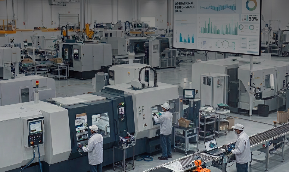
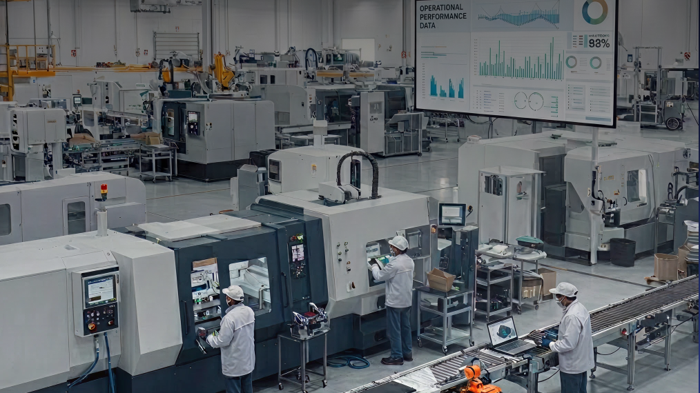
How Elecbits Simplifies PCB Manufacturing for Hardware Companies
A lot of hardware manufacturing delays don't actually start on the factory floor. They usually begin earlier with sourcing gaps, supplier miscommunication, or BOM issues that no one notices until production slows down.
Elecbits helps hardware teams avoid that by bringing PCB development, sourcing, assembly, embedded engineering and production management together into one connected workflow instead of having to manage multiple vendors and endless spreadsheets.
The company also developed Elecbits XOR, an AI-powered platform that provides teams visibility into component pricing, availability, alternate parts and sourcing risks ahead of becoming manufacturing problems.
That's why companies like Motherson, Maruti Suzuki, Siemens and Ola Electric depend on Elecbits for electronics manufacturing support.
Conclusion
The manufacturing of PCBs goes beyond just the printing of electronic circuits onto the board; it encompasses material science, engineering, quality control, and logistics – all integrated in a tightly controlled process.
Knowing how PCBs are manufactured helps hardware companies to have more control over product quality, manufacturing time, and production cost. It also improves communication with fabrication partners and assembly vendors.
As electronics devices are becoming smaller, smarter, and more connected, the ability to manage PCB manufacturing effectively is becoming a core competitive advantage.

 QUALITY & CONSISTENCY Quality standards Reliable methods to keep our quality consistent.INSIGHTS Blog Deep dive into market-moving trends


